logo
Datasheet4U.com - FDC6322C
logo

FDC6322C Datasheet, FET, Fairchild Semiconductor

FDC6322C Datasheet, FET, Fairchild Semiconductor

FDC6322C

datasheet Download (Size : 96.76KB)

FDC6322C Datasheet
FDC6322C

datasheet Download (Size : 96.76KB)

FDC6322C Datasheet

FDC6322C Features and benefits

FDC6322C Features and benefits

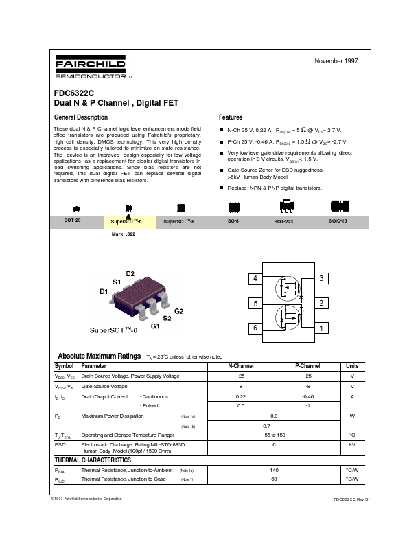
N-Ch 25 V, 0.22 A, RDS(ON) = 5 Ω @ VGS= 2.7 V. P-Ch 25 V, -0.46 A, RDS(ON) = 1.5 Ω @ VGS= -2.7 V. Very low level gate drive requirements allowing direct operation in 3 V .

FDC6322C Application

FDC6322C Application

as a replacement for bipolar digital transistors in load switching applications. Since bias resistors are not required, .

FDC6322C Description

FDC6322C Description

These dual N & P Channel logic level enhancement mode field effec transistors are produced using Fairchild's proprietary, high cell density, DMOS technology. This very high density process is especially tailored to minimize on-state resistance. The d.

Image gallery

FDC6322C Page 1 FDC6322C Page 2 FDC6322C Page 3

TAGS

FDC6322C
Dual
Channel
Digital
FET
Fairchild Semiconductor

Manufacturer


Fairchild Semiconductor

Related datasheet

FDC6320C

FDC6321C

FDC6323L

FDC6324L

FDC6325L

FDC6326L

FDC6327C

FDC6329L

FDC6301N

FDC6302P

FDC6303N

FDC6304P

FDC6305N

Since 2006. D4U Semicon.   |   Datasheet4U.com   |   Contact Us   |   Privacy Policy   |   Purchase of parts